Monthly Archives: July 2011
Here are examples of materials we tested this month:
Mechanical:
• Nano fracture of ceramic
• Nano scratch of microelectronic coating
• Nano scratch of medical coating
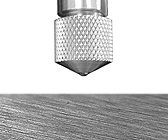
• Nano compression of micro feature
• Nano stress strain solar film
• Micro scratch of TiN coating
• Microindentation of concrete
3D Non-Contact Profilometry:
• Texture patterns of fracture
• Flatness of flip chip
• Planarity of microelectronic
• Profile of dental samples
• Roughness of micro pitting
• Roughness of micro medical parts
• Step Height of solder paste
• Coefficient of friction polyurethane coating
• Coefficient of friction medical plastic
• 24hr Wear resistance of coated glass
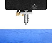
• Wear resistance of submerged implant
• chrome carbide coating wear resistance